

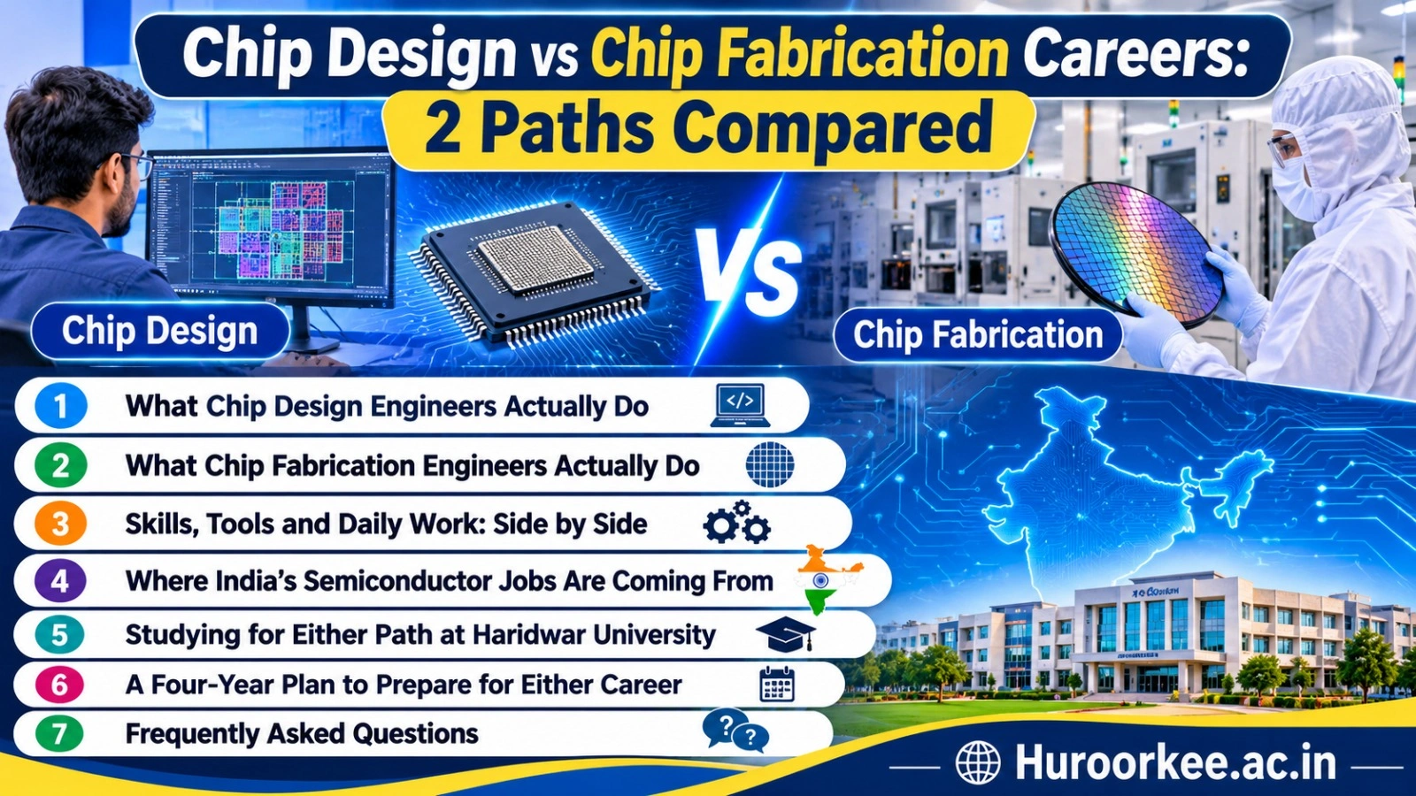
Chip Design vs Chip Fabrication Careers: 2 Paths Compared
Mr. Jitendra Chaudhary
Admissions Manager, Haridwar University
Chip Design vs Chip Fabrication Career paths is a choice almost every electronics student faces, often after hearing that semiconductors are the future without anyone saying which part of the chip business they mean. Both paths end in the same tiny piece of silicon inside a phone, a car, or a hospital scanner. The daily work, however, looks nothing alike. One path is mostly screens, code, and simulation. The other involves cleanroom suits, chemicals, and heavy process equipment. This guide compares the two plainly, shows what Indian government sources say about demand, and explains how a student can prepare for either route at Haridwar University.
Table of Contents
- 1. What Chip Design Engineers Actually Do
- 2. What Chip Fabrication Engineers Actually Do
- 3. Skills, Tools and Daily Work: Side by Side
- 4. Where India’s Semiconductor Jobs Are Coming From
- 5. Studying for Either Path at Haridwar University
- 6. A Four-Year Plan to Prepare for Either Career
- 7. Frequently Asked Questions (FAQs)
1. What Chip Design Engineers Actually Do
Chip design is the work of deciding what a microchip should do and turning that architectural concept into a physical layout that a manufacturing foundry can build. It moves through sequential, interdependent engineering stages:
- System Architecture: System architects define processor instruction sets, cache hierarchies, bus protocols, and power-performance-area (PPA) trade-offs.
- RTL Design: Front-end engineers describe logic behavior using Hardware Description Languages (HDL) such as Verilog, SystemVerilog, or VHDL.
- Verification & Emulation: Design Verification (DV) engineers write testbenches using Universal Verification Methodology (UVM) to find obscure corner-case bugs before tape-out.
- Physical Design: Back-end engineers handle floorplanning, place-and-route (P&R), clock tree synthesis (CTS), static timing analysis (STA), and design rule checking (DRC).
- Analog & Mixed-Signal Layout: Specialists design Phase-Locked Loops (PLLs), Analog-to-Digital Converters (ADCs), and high-speed I/O interfaces.
Most of this work happens on high-performance UNIX workstations using Electronic Design Automation (EDA) software suites (such as Synopsys, Cadence, and Siemens EDA). Patience with complex logic debugging and timing closure matters far more than physical workshop skills.
Government Backing for Design
India’s Design Linked Incentive (DLI) scheme, spearheaded by the India Semiconductor Mission (ISM), provides financial reimbursements and access to advanced EDA tool infrastructure for integrated circuits, system-on-chips (SoCs), and IP cores. The national goal is to nurture domestic chip-less fabless start-ups so that intellectual property is created inside India.
2. What Chip Fabrication Engineers Actually Do
Fabrication begins where design ends. A semiconductor fabrication plant (fab) turns a validated GDSII layout into functional silicon dies by printing hundreds of intricate microscopic layers onto an ultra-pure monocrystalline silicon wafer inside a Class 1 cleanroom.
Roles Inside the Fab
- Process Engineers: Tune and oversee chemical vapor deposition (CVD), extreme ultraviolet (EUV) or deep ultraviolet (DUV) photolithography, plasma etching, and high-energy ion implantation.
- Equipment Engineers: Maintain billion-dollar vacuum chambers, laser steppers, turbo-pumps, and robotic wafer handling tracks to ensure zero unplanned downtime.
- Yield & Defect Metrology Engineers: Inspect wafer defects using scanning electron microscopes (SEM) and statistical process control (SPC) algorithms to maximize good die per wafer.
When an etching tool drifts by a single nanometer, an entire batch of hundreds of wafers worth millions of rupees can be scrapped. Fab engineers learn to monitor sensor data obsessively and act instantly. Teams combine electronics, physics, chemical, materials, and mechanical engineering graduates.
Fabrication versus Packaging (ATMP / OSAT)
Students often conflate fabrication with packaging, but they are distinct career tracks. A Press Information Bureau (PIB) release highlights projects across both: a compound semiconductor fabrication plant at Dholera and an Assembly, Testing, Marking, and Packaging (OSAT) plant at Surat, both in Gujarat. Packaging takes diced wafers, attaches lead frames or substrate balls, encapsulates them in protective resin, and validates reliability under thermal stress. To explore the wider manufacturing workforce demand, read our companion analysis on Semiconductor Manufacturing Jobs in India: The Talent Gap.
3. Skills, Tools and Daily Work: Side by Side
The clearest way to compare Chip Design vs Chip Fabrication Career paths is to contrast a typical working day. A chip designer spends their day reading logic waveforms, scripting testbench regressions in Python or Perl, and closing timing violations. A fabrication engineer spends their day analyzing chamber telemetry, inspecting cleanroom tool alarms, adjusting recipe chemistry, and coordinating with floor technicians.
| Comparison Factor | Chip Design | Chip Fabrication |
|---|---|---|
| Primary Mission | Architecting how a circuit behaves, writing RTL code, and laying out transistors. | Building the physical microchip layer by layer on silicon wafers with nanometer precision. |
| Work Environment | Office design centre, dual-monitor UNIX workstations, flexible desk hours. | Fab floor, positive-pressure cleanroom suites (bunny suits), often round-the-clock shift cycles. |
| Core Subjects | Digital electronics, CMOS VLSI, computer architecture, algorithms, and timing analysis. | Solid-state device physics, chemical thermodynamics, thin films, vacuum systems, and material science. |
| Primary Tool Suites | EDA suites (Cadence Innovus/Virtuoso, Synopsys Design Compiler, Mentor Questa), SystemVerilog, Python. | Photolithography steppers, plasma etchers, spectroscopic ellipsometers, SEM, JMP/Minitab statistical tools. |
| Initial Entry Roles | RTL Design Engineer Trainee, Design Verification Engineer, Physical Design Trainee. | Junior Process Engineer, Equipment Maintenance Engineer, Fab Yield Specialist. |
| Best Suited For | Students who enjoy discrete logic, coding, mathematical puzzles, and software-driven hardware design. | Students passionate about applied physics, experimental chemistry, physical machinery, and high-tech manufacturing. |
For a detailed breakdown of career opportunities across the broader semiconductor ecosystem, see our comprehensive guide on Semiconductor & VLSI Careers in India.
4. Where India’s Semiconductor Jobs Are Coming From
Official data reveals concrete industrial mobilization. A Press Information Bureau release dated 5 May 2026 confirmed that approved projects under the India Semiconductor Mission have reached 12 units, representing a cumulative capital outlay exceeding ₹1.64 lakh crore. Ten projects are in active construction, and two have initiated commercial silicon shipments. The two newest units alone will generate 2,230 high-skill engineering jobs.
On the design side, the Ministry of Electronics and IT (MeitY) reports that the Chips to Startups (C2S) programme is actively working toward its 10-year goal of training 85,000 semiconductor engineers across 315 academic institutions and 104 hardware start-ups. Students should note the geographic distribution: wafer fabrication and ATMP units are heavily clustered in dedicated industrial zones like Dholera, Sanand, and Morigaon, whereas chip design centers operate across major tech hubs including Bengaluru, Hyderabad, Noida, Pune, and Chennai.
5. Studying for Either Path at Haridwar University
Roorkee College of Engineering at Haridwar University provides an integrated four-year pathway through its B.Tech. Hons. ECE with AI (VLSI Certification from IIT/NIT). The curriculum pairs classical circuit theory with advanced digital VLSI, verification testbenches, and EDA simulation tools. Read our detailed programme guide to B.Tech ECE with VLSI Certification for semester-by-semester details. For students seeking advanced research in device physics, the university also offers an M.Tech. in Electronics and Communication Engineering.
Eligibility & Transparent Fee Structure
Admission requires 10+2 with Physics, Chemistry, and Mathematics (minimum 50% aggregate, 45% for SC/ST) and a valid score in JEE Main or state entrance exams. As published on the official Fees & Scholarships page for the 2027-28 session, the transparent fee schedule is outlined below:
| Programme | Annual Tuition | 1st Year Total | 2nd Year | 3rd Year | 4th Year |
|---|---|---|---|---|---|
| B.Tech. Hons. ECE with AI (VLSI) | ₹62,000 | ₹1,32,000 | ₹1,15,000 | ₹1,15,000 | ₹1,15,000 |
| M.Tech. ECE | ₹45,000 | ₹78,000 | ₹70,000 | — | — |
Hostel fees cover lodging, three daily meals, and laundry: ₹85,000 (Standard), ₹95,000 (Semi-Deluxe), and ₹1,05,000 (Deluxe AC). Transparent merit scholarships grant 80%, 50%, 20%, or 10% on first-year tuition based on JEE Main ranks or Class 12 PCM marks, alongside a dedicated 25% waiver for female students.
6. A Four-Year Plan to Prepare for Either Career
Do not attempt to specialize too early. A structured roadmap ensures strong options regardless of how the industry evolves:
- Years 1 & 2 (Foundations First): Build unassailable command over circuit theory, semiconductor physics, digital logic, and basic programming (C/Python and basic Verilog). Both fab and design managers value solid foundational logic.
- Year 3 (Choose Your Trajectory): Design-leaning candidates should select advanced RTL design, STA, and verification electives; fabrication-leaning candidates should focus on materials science, solid-state microelectronics, and cleanroom vacuum technology.
- Year 4 (Tangible Capstone Proof): Complete an industry-grade capstone project. A verified RISC-V core or AXI bus interface proves design competence, while a semiconductor device simulation (TCAD) or wafer defect study proves fabrication interest.
Throughout your study, Haridwar University’s Student Welfare Service provides comprehensive student mentorship through Student Care Centres with a 24-hour query response commitment. Prospective applicants should review the admission overview for complete registration steps, and review the Placement Overview for campus recruitment partners.
7. Frequently Asked Questions (FAQs)
1. Which is better, chip design or chip fabrication?
Neither is objectively superior. Chip design suits engineers who love logic architectures, coding, and screen-based simulation. Chip fabrication suits those intrigued by applied physics, chemical reactions, heavy machinery, and physical plant operations.
2. Can an ECE student work in semiconductor fabrication?
Yes. Commercial fab engineering teams regularly combine electronics, physics, chemical, mechanical, and materials engineers. Strong knowledge of semiconductor devices gives ECE graduates an excellent base for process engineering roles.
3. Is a master's degree compulsory for chip design?
No. Many entry-level RTL design and design verification (DV) roles actively recruit B.Tech graduates with strong digital logic and Verilog fundamentals. An M.Tech is primarily advantageous for specialized analog RF layout or deep physical design roles.
4. What is OSAT, and is it design or fabrication?
OSAT stands for Outsourced Semiconductor Assembly and Test. It encompasses packaging and testing of fabricated silicon dies. It occurs downstream of wafer fabrication, making it a distinct manufacturing discipline.
5. Does the government support chip design careers?
Yes. MeitY’s Chips to Startups (C2S) programme is actively funding EDA tool access and aims to train 85,000 design engineers over a 10-year horizon, supported by the Design Linked Incentive (DLI) scheme.
6. Which HU programme suits a VLSI-focused student?
The B.Tech. Hons. ECE with AI (VLSI Certification from IIT/NIT) offered by Roorkee College of Engineering at Haridwar University provides targeted preparation. The college also offers an M.Tech. ECE for advanced postgraduate studies.
7. What is the fee for B.Tech ECE with AI at Haridwar University?
The official fee structure lists an annual tuition of ₹62,000, bringing the first-year comprehensive total to ₹1,32,000 (including admission, exam, and uniform charges), and ₹1,15,000 annually for years 2 through 4.
8. Which scholarships can a first-year student receive?
First-year tuition waivers of 10% to 80% are awarded based on JEE Main ranks and Class 12 PCM percentages. Additional 25% waivers are provided to female applicants, along with sports-quota concessions.
9. How do I apply and confirm a seat?
Students can register online via huroorkee.ac.in/apply-now or visit the Roorkee campus. Initial seat confirmation requires a registration deposit of ₹25,000 via DD, NEFT, or online payment.
Ready to Advance Your Education at Haridwar University?
Launch your career in semiconductor engineering, VLSI design, and advanced electronics. Explore our specialized B.Tech ECE programme with IIT/NIT certification and transparent merit scholarships. Applications are open for the 2027-28 session.