

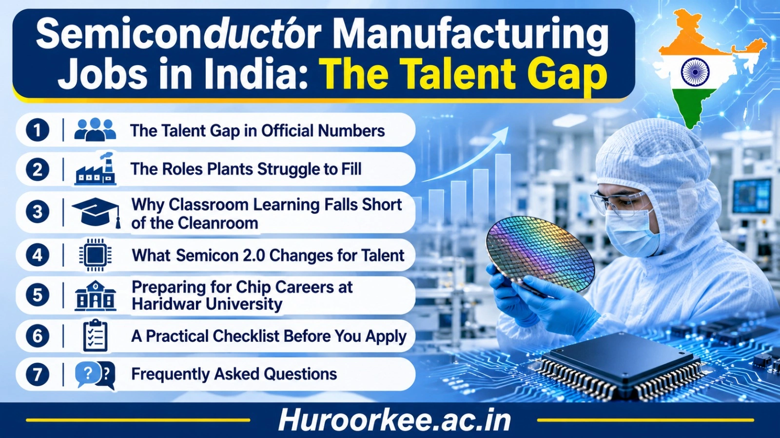
Semiconductor Manufacturing Jobs in India: The Talent Gap
Dr Aadesh K. Arya
Pro Vice-Chancellor, Haridwar University
Semiconductor Manufacturing Jobs in India are no longer a promise on paper. The Government of India has approved twelve manufacturing units, and five are already in commercial production. Even so, the people who will run cleanrooms, tune etching steps, and test finished chips are still being trained. Talent is one of the six pillars of the new Semicon 2.0 scheme for exactly that reason. Official data checked on 16 November 2026 shows where the gap sits and what an aspiring student can do about it.
Table of Contents
- 1. The Talent Gap in Official Numbers
- 2. The Roles Plants Struggle to Fill
- 3. Why Classroom Learning Falls Short of the Cleanroom
- 4. What Semicon 2.0 Changes for Talent
- 5. Preparing for Chip Careers at Haridwar University
- 6. A Practical Checklist Before You Apply
- 7. Frequently Asked Questions (FAQs)
1. The Talent Gap in Official Numbers
In 2021 India had no commercial silicon chip plant. According to the Press Information Bureau (PIB) backgrounder of 17 September 2026, twelve manufacturing units are now approved and five are in commercial production. That leaves seven plants currently under active construction, each requiring engineers, technicians, and cleanroom operators from day one.
| Indicator | Latest Official Figure | Source |
|---|---|---|
| Manufacturing units approved | 12 | PIB backgrounder, 17 Sep 2026 |
| Units in commercial production | 5 | PIB backgrounder, 17 Sep 2026 |
| Cumulative investment approved | Over ₹1.64 lakh crore | PIB backgrounder, 17 Sep 2026 |
| Semicon 2.0 outlay (approved 15 July 2026) | ₹1,27,500 crore | PIB backgrounder, 17 Sep 2026 |
| Engineers with chip-design tool access | More than 1 lakh | PIB backgrounder, 17 Sep 2026 |
| Projected global shortage by 2030 | 1,000,000 professionals | Union IT Minister, AIR, 29 Aug 2025 |
The official data highlights a clear structural imbalance. India employs nearly 20% of the world's chip design workforce, but domestic wafer fabrication and packaging are described as nascent. Design talent surged ahead because it requires high-end workstations, Electronic Design Automation (EDA) software, and strong mathematical training. Fabrication and packaging talent, by contrast, requires operating physical plants that are only now beginning commercial runs.
2. The Roles Plants Struggle to Fill
Semiconductor manufacturing is an unforgiving, multi-stage precision sequence. Inside fabrication facilities (fabs), wafers pass through chemical vapor deposition, photolithography, plasma etching, and ion implantation, followed by assembly, testing, marking, and packaging (ATMP/OSAT) units.
| Role Inside Plant | What the Work Involves | Usual Academic Starting Point |
|---|---|---|
| Process Engineer | Controls cleanroom process parameters across chemical deposition, lithography, dry/wet etching, and thermal annealing. | Degree in Electronics, Chemical, or Materials streams |
| Equipment Technician or Operator | Maintains high-vacuum chambers, laser steppers, robotics, and cleanroom air handling systems on the fab floor. | Technical Diploma or Degree plus hands-on industrial training |
| Packaging and Test Engineer | Oversees die attachment, wire bonding, flip-chip packaging, thermal stress testing, and automated test equipment (ATE). | Degree in Electronics or Mechanical Engineering |
| Design and Verification Engineer | Architects digital and analog integrated circuits, writes RTL code (SystemVerilog), and performs pre-silicon verification. | Electronics Degree with dedicated VLSI training |
The Union Minister for Electronics and IT noted that the world faces a shortage of one million semiconductor professionals by 2030. India cannot rely on importing experienced cleanroom talent from Taiwan, Japan, or the US. To understand how VLSI design and semiconductor fabrication intersect, read our detailed analysis on Semiconductor & VLSI Careers in India: The Opportunity Explained.
3. Why Classroom Learning Falls Short of the Cleanroom
Design Tools Travelled Faster Than Fab Tools
More than 1 lakh engineers across 500 organisations—including 400 academic institutions and 100 start-ups—now have access to advanced EDA chip-design tools under government-supported programmes. These organisations have developed over 300 chip designs. Software licenses can be distributed instantly over the cloud. A physical Class 1 or Class 100 cleanroom, costing billions of dollars, cannot. Consequently, a graduate can master circuit simulation without ever experiencing cleanroom protocols, particulate filtration, or toxic gas handling.
What a University Can Realistically Deliver
A university cannot replace a commercial fabrication facility, but it can instill the rigorous electronics fundamentals, digital design flows, and obsessive verification habits that plant operators require on day one. Haridwar University, established in 2010 in Roorkee, delivers engineering programmes designed to bridge this divide through practical lab work and industry-standard verification curricula.
4. What Semicon 2.0 Changes for Talent
The Union Cabinet approved Semicon 2.0 on 15 July 2026 with an outlay of ₹1,27,500 crore across six comprehensive pillars, with talent development occupying center stage. According to the India Semiconductor Mission (ISM), this pillar aims to build a multi-tiered talent pipeline:
- Shop-Floor Operators & Technicians: Standardized hands-on polytechnic curricula for tooling and vacuum maintenance.
- Undergraduate Engineers: Specialized B.Tech coursework integrating VLSI design, semiconductor physics, and automated testing.
- Postgraduate & Doctoral R&D: Advanced fellowships in materials science, lithography chemistry, and wide-bandgap semiconductors (SiC, GaN).
Supported training initiatives run for up to six years, providing sustained institutional backing to cultivate homegrown plant leadership.
5. Preparing for Chip Careers at Haridwar University
Haridwar University offers a targeted undergraduate pathway through its B.Tech. Hons. ECE with AI (VLSI Certification from IIT/NIT). The four-year curriculum spans digital system design, microprocessors, embedded firmware, AI/ML hardware accelerators, industry-standard EDA simulation, and hardware verification labs. You can also explore our dedicated guides on B.Tech ECE with AI and VLSI Certification and B.Tech ECE careers in 5G, IoT, and semiconductors.
Applicants require 10+2 with Physics, Chemistry, and Mathematics (PCM) and at least 50% aggregate marks (45% for SC/ST candidates), alongside a valid score in JEE Main or state entrance examinations.
Fee Structure (B.Tech. Hons. ECE with AI)
As per the official Fee Structure 2026-27 published on the Fees & Scholarships page, fees include tuition, enrolment, admission, examination, and uniform fees. Transport and hostel charges are separate:
| Academic Period | Amount (₹) |
|---|---|
| 1st Year, Semester 1 | ₹96,000 |
| 1st Year, Semester 2 | ₹36,000 |
| 1st Year Total | ₹1,32,000 |
| 2nd Year | ₹1,15,000 |
| 3rd Year | ₹1,15,000 |
| 4th Year | ₹1,15,000 |
Merit Scholarships on First-Year Tuition
| JEE Main Rank | Class 12 PCM % | CUET Percentile | Tuition Waiver |
|---|---|---|---|
| 1 to 1,00,000 | Above 90% | Above 90% | 80% Scholarship |
| 1,00,001 to 2,00,000 | Above 80% up to 90% | Above 80% up to 90% | 50% Scholarship |
| 2,00,001 to 3,00,000 | Above 70% up to 80% | Above 70% up to 80% | 20% Scholarship |
| 3,00,001 to 6,00,000 | Above 60% up to 70% | Above 60% up to 70% | 10% Scholarship |
In addition, female applicants receive a dedicated 25% first-year tuition scholarship, and sports quota holders receive waivers between 10% and 50%. A student can hold only one scholarship scheme.
6. A Practical Checklist Before You Apply
Before committing to an electronics or chip-oriented degree, verify these operational checkpoints:
- Examine Academic Eligibility: Confirm PCM percentage prerequisites and entrance exam submission dates.
- Inspect Simulation Labs: Ask which EDA tool suites (Cadence, Synopsys, Mentor, or open-source equivalents) and FPGA development boards are integrated into the practical curriculum. Explore programmes under Roorkee College of Engineering.
- Verify Total Outlay & Housing: Account for tuition, uniforms, and hostel costs. Haridwar University lists hostel boarding at ₹85,000 for standard rooms, ₹95,000 for semi-deluxe, and ₹1,05,000 for AC deluxe rooms, including lodging, mess, and laundry.
- Review Student Support Infrastructure: Haridwar University's Student Welfare Service operates Student Care Centres across academic blocks with a 24-hour turnaround commitment. Review our Training and Placement Overview to understand recruiter engagement.
Treat your undergraduate journey as a disciplined multi-year build-up: master semiconductor theory and VLSI architecture first, seize specialized cleanroom training programs as new plants scale up, and align your final-year projects with commercial manufacturing requirements.
7. Frequently Asked Questions (FAQs)
1. Why can't semiconductor plants find enough skilled people?
The plants are entirely new. India developed a substantial chip design workforce over the past two decades, but domestic fabrication and packaging lines are at a nascent stage. Hands-on experience operating cleanrooms and high-vacuum equipment remains scarce.
2. How big is the talent shortage?
The Union IT Minister has stated that the world faces a projected deficit of one million semiconductor professionals by 2030. Official government sources do not publish an isolated India-only vacancy figure, so realistic workforce training remains a shared national priority.
3. Which roles are hardest to fill?
While no official ranking exists, the Semicon 2.0 talent pillar targets four distinct operational layers: circuit design engineers, fabrication process engineers, ATMP packaging specialists, and shop-floor technicians.
4. Are design jobs easier to get than manufacturing jobs?
Design jobs have a two-decade head start because India already houses nearly 20% of global design engineers. Commercial manufacturing positions will expand progressively as newly approved fabrication and packaging plants commission their commercial lines.
5. Does a B.Tech in ECE qualify me for chip roles?
Yes, an ECE degree provides the mandatory foundational principles in electronics, semiconductors, and microprocessors. However, specialized plant and cleanroom roles also require process-specific hands-on training.
6. What is the eligibility for B.Tech. Hons. ECE with AI at Haridwar University?
Candidates must have completed 10+2 with PCM, scoring at least 50% in Physics, Chemistry, and Mathematics (45% for SC/ST), plus a valid score in JEE Main or state entrance exams.
7. What does the programme cost?
As per the official Fee Structure 2026-27, the first year is ₹1,32,000 (₹96,000 in Semester 1 and ₹36,000 in Semester 2). Years two through four are ₹1,15,000 annually. Transport is billed separately.
8. Which scholarships can a first-year student receive?
Merit scholarships of 80%, 50%, 20%, or 10% on first-year tuition are tied to JEE Main ranks, Class 12 PCM scores, or CUET percentiles. Female students receive a 25% tuition scholarship.
9. What hostel and student support facilities are available?
Hostel charges are ₹85,000 (standard), ₹95,000 (semi-deluxe), and ₹1,05,000 (AC deluxe), covering lodging, mess, and laundry. Student Care Centres in each block resolve queries within 24 hours.
Ready to Advance Your Education at Haridwar University?
Prepare for high-growth opportunities in semiconductor technology, embedded systems, and VLSI design. Explore our industry-aligned B.Tech ECE programme with dedicated labs and merit scholarships. Applications are open for the 2027-28 academic session.