

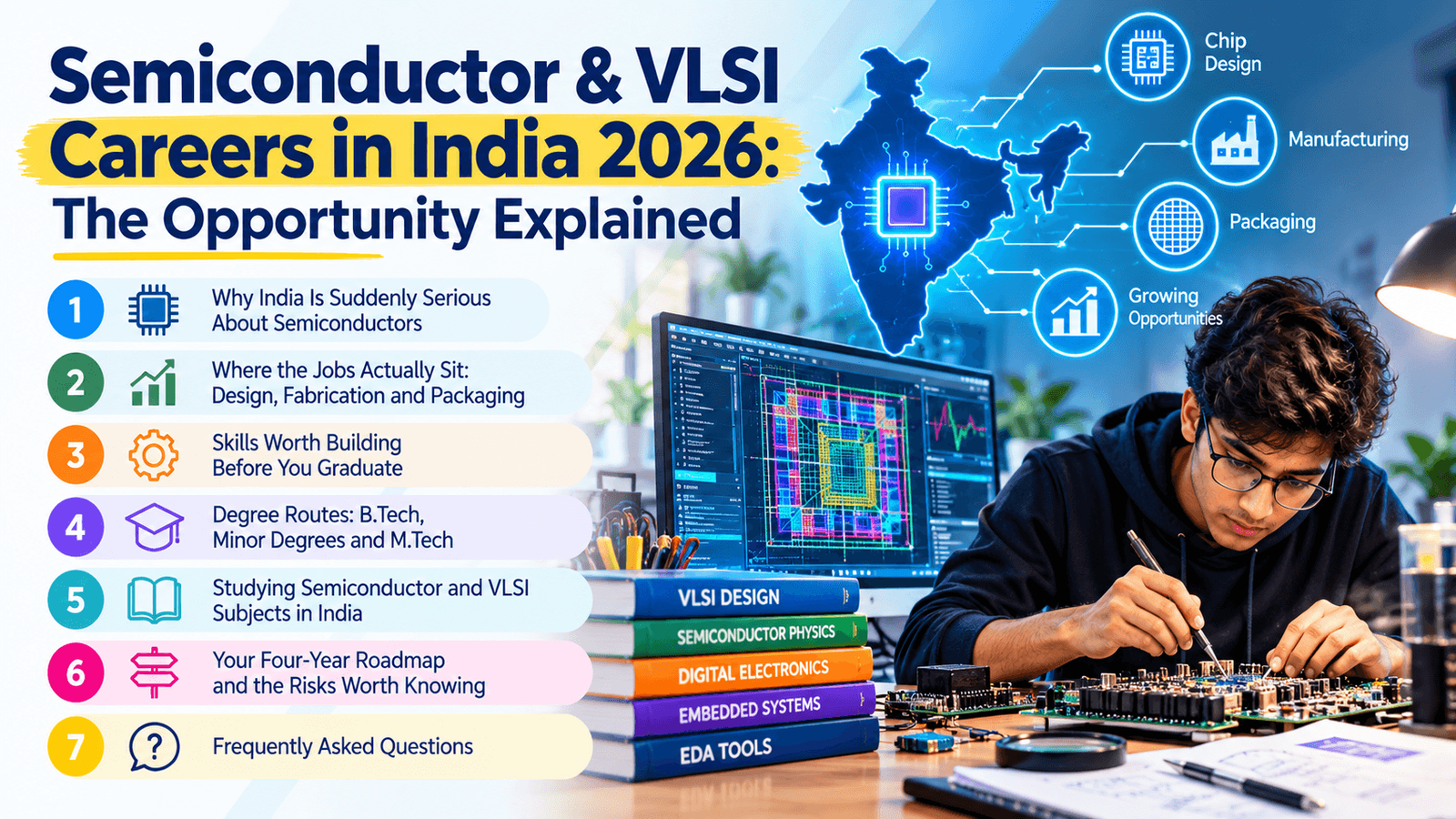
Semiconductor & VLSI Careers in India 2026 are being shaped by public capital and industrial policy on a scale earlier batches of electronics engineering students simply did not see. Commercial fabrication plants, advanced packaging units (ATMP/OSAT), and chip-design startups now enjoy decisive government backing, and that transforms what a B.Tech in Electronics & Communication Engineering can lead to.
This comprehensive roadmap covers macroeconomic industry tailwinds, the distinct functional domains within semiconductor manufacturing, core technical skills to cultivate, and where degree programmes at Haridwar University in Roorkee fit. Every figure cited traces directly to official policy releases, such as the government's India Semiconductor Mission 2.0 (ISM) backgrounder.
Table of Contents
- 1. Why India Is Suddenly Serious About Chips
- 2. Where the Jobs Actually Sit: Design, Fabrication and Packaging
- 3. Skills Worth Building Before You Graduate
- 4. Degree Routes: B.Tech, Minor Degrees and M.Tech
- 5. Studying Semiconductor and VLSI Subjects at Haridwar University
- 6. Your Four-Year Roadmap and the Risks Worth Knowing
- 7. Frequently Asked Questions (FAQs)
- 8. Build Your Future in India's Silicon Revolution
1. Why India Is Suddenly Serious About Chips
Microchips power everything: smartphones, electric vehicles, telecommunication base stations, aerospace guidance, renewable energy grids, and high-performance AI accelerators. The global supply disruptions of recent years laid bare the extreme vulnerability of concentrated chip manufacturing.
According to official PIB data, chip shortages disrupted operations across more than 169 international industries. Moreover, Taiwan alone produces over 60% of the world's semiconductors and nearly 90% of sub-7nm advanced nodes. In response, the Government of India launched the India Semiconductor Mission (ISM) in December 2021 with a ₹76,000 crore fiscal incentive framework providing up to 50% project cost support on a pari-passu basis.
The operational momentum is substantial:
- By December 2025, ten major commercial projects representing a combined cumulative investment of ₹1.60 lakh crore had been sanctioned across six Indian states.
- Budget 2026–27 subsequently introduced ISM 2.0 with a fresh initial budgetary outlay of ₹1,000 crore to expand indigenous equipment, raw material, and specialty chemicals capacity.
- India's domestic semiconductor market—valued at approximately $38 billion in 2023—is projected by industry assessments cited by PIB to surge past $100 to $110 billion by 2030.
Crucially, India already serves as a global powerhouse in front-end design. Under the Design Linked Incentive (DLI) scheme, India accounts for roughly 20% of the world's semiconductor design workforce, with 24 indigenous fabless chip startups receiving direct fiscal support by early 2026.
2. Where the Jobs Actually Sit: Design, Fabrication and Packaging
Careers in the semiconductor domain are not monolithic. They span three distinct industrial sub-sectors with very different day-to-day engineering responsibilities:
1. Chip Design & Verification (VLSI / Fabless)
Very Large Scale Integration (VLSI) involves embedding hundreds of millions of transistors into silicon architecture. Logic design engineers code RTL (Register Transfer Level) using Verilog/SystemVerilog; functional verification engineers stress-test the design to eliminate errant logic before manufacturing; and physical design engineers map logical schematics into nanometer physical layouts (GDSII). This segment employs the largest share of Indian electronics talent.
2. Wafer Fabrication & Process Engineering (Foundries)
Fabrication plants ("fabs") are capital-intensive cleanroom factories that etch physical microstructures onto pure silicon or silicon carbide (SiC) wafers. Approved projects include the Tata Electronics mega-fab in Dholera, Gujarat (built in partnership with Taiwan's PSMC). Core roles focus on photolithography, thin-film chemical deposition, plasma etching, and yields engineering.
3. Assembly, Testing, Marking & Packaging (ATMP / OSAT)
After circular wafers are sliced into individual dies, ATMP/OSAT facilities encase them in protective thermal packages and conduct rigorous electrical testing. Global players like Micron Technology (Sanand facility for DRAM and NAND memory), CG Power, and Kaynes Technology operate in this segment. It requires hardware testing, quality assurance, automation, and process control specialists.
The trajectory you pursue depends heavily on college training and campus placement connections. Prospective students can examine Haridwar University's verified corporate placement overview to observe institutional recruiting partners and career services.
3. Skills Worth Building Before You Graduate
Breaking into high-paying VLSI design and semiconductor careers demands technical proficiencies far beyond basic textbook memorization:
- Electronics Fundamentals: Rigorous command of digital logic design, CMOS analog circuits, semiconductor physics, and timing analysis.
- Hardware Description Languages (HDLs): Fluency in Verilog, SystemVerilog, and UVM (Universal Verification Methodology), the standard language of global semiconductor design teams.
- Electronic Design Automation (EDA) Tools: Industry-standard software suites (Cadence, Synopsys, Siemens/Mentor Graphics) used for logic synthesis, static timing analysis (STA), and physical layout verification.
- Scripting & Automation: Linux shell scripting, Python, and Tcl (Tool Command Language) to automate EDA simulation pipelines.
National initiatives actively bridge the laboratory software gap. Under the Ministry of Electronics & Information Technology's (MeitY) Chips to Startup (C2S) Programme, centralized EDA tool support has reached 397 universities and startups (check C2S supported institutions), enabling students from 46+ institutions to fabricate 56 tape-outs at the SCL foundry in Mohali.
Additionally, NIELIT Calicut's SMART Lab Programme offers remote laboratory access and specialized VLSI certifications, having trained more than 62,000 engineers toward its national target of 100,000 professionals.
4. Degree Routes: B.Tech, Minor Degrees and M.Tech
The standard academic entry route is a four-year Bachelor of Technology in Electronics & Communication Engineering (ECE) or Electrical Engineering.
To match the semiconductor boom, the All India Council for Technical Education (AICTE) introduced a dedicated Model Curriculum for Minor Degrees in VLSI Design & Technology, diploma pathways in IC manufacturing, and specialized curricula that engineering colleges across India are integrating.
While an M.Tech in VLSI or Microelectronics historically represented the standard entry requirement for Tier-1 multinational design teams, industry demand has broadened significantly: a B.Tech graduate possessing demonstrable FPGA design projects, clean RTL code samples, and tape-out or EDA tool familiarity can secure entry-level design, testing, or field applications roles.
For an in-depth breakdown of undergraduate curriculum choices, read Haridwar University's dedicated guide to the B.Tech ECE with AI & VLSI Certification Programme.
5. Studying Semiconductor and VLSI Subjects at Haridwar University
The Roorkee College of Engineering at Haridwar University offers specialized undergraduate and postgraduate programmes designed for the evolving hardware landscape, notably the B.Tech. Hons. ECE with AI (VLSI Certification from IIT/NIT) and the advanced M.Tech in Electronics & Communication Engineering.
Established in 2010, Haridwar University features a 20-acre modern campus on the banks of the Ganga Canal in Roorkee, equipped with dedicated electronics laboratories and advanced computing facilities.
Here is the verified fee structure for electronics engineering programmes at Haridwar University:
Source: Verified from Haridwar University Fee Structure 2026-27. Figures include tuition, enrollment, admission, examination, and uniform charges. Transport and hostel accommodation are charged separately.
Scholarship Architecture & Financial Support: HU awards substantial first-year tuition waivers based on academic merit:
- Merit Concessions: 80% waiver on tuition for Class 12 PCM/JEE scores above 90%, scaling down to 10% for 60–70% marks bands.
- Girls' Education Concession: 25% first-year tuition waiver for female students.
- Semester Academic Excellence: ₹5,000 cash award for students scoring 85%+ in semester exams on their first attempt.
- GATE Scholarships: M.Tech candidates qualifying GATE-2026 are eligible for AICTE financial assistance. Review our GATE preparation guide for strategy insights.
6. Your Four-Year Roadmap and the Risks Worth Knowing
Success in semiconductor engineering requires a systematic multi-year progression:
• Years 1 & 2 (Foundations): Master network analysis, analog and digital electronics, CMOS devices, and C/Python programming.
• Year 3 (Specialisation): Learn Verilog/SystemVerilog, implement designs on FPGA evaluation boards (Xilinx/Altera), and complete online EDA simulations.
• Year 4 (Capstone & Industrial Exposure): Build an end-to-end SoC or ASIC verification project and pursue internships (see our guide on B.Tech internships at Haridwar University).
Industry Realities & Timelines: It is equally important to balance enthusiasm with realism. Fabs and advanced packaging units require multi-year construction and qualification cycles before reaching peak operational capacity. The official PIB backgrounder notes projected direct job creation from initial projects at approximately 1,500 roles in fabs, 3,000 in packaging units, and 200 in DLI design startups by 2026–27. This is a durable, long-horizon industry—plan your skill architecture for the decade ahead, not just the upcoming quarter.
Administrative support at HU is streamlined through the Student Welfare Service, with dedicated Student Care Centres in each academic block ensuring prompt 24-hour resolution of academic and administrative requests. Details on eligibility, counselling, and entrance evaluations are accessible on the HU Admission Overview portal.
7. Frequently Asked Questions (FAQs)
What does a VLSI engineer actually do?
A VLSI engineer designs, simulates, verifies, and layouts integrated circuits containing millions of transistors. The workflow spans front-end architecture, RTL coding in Verilog, functional verification with SystemVerilog/UVM, static timing analysis (STA), and physical backend place-and-route.
Is a B.Tech in ECE enough to get started?
Yes. While postgraduate degrees provide specialized depth, a B.Tech in Electronics & Communication Engineering accompanied by practical Verilog proficiency, FPGA hardware demonstrations, and EDA tool projects represents a valid pathway into entry-level chip design, verification, and testing roles.
Do I need an M.Tech?
No mandatory regulatory requirement exists. However, an M.Tech in ECE/VLSI offers advanced exposure to complex sub-micron architectures, RF design, and research tape-outs. Haridwar University provides an M.Tech in ECE at ₹78,000 for Year 1 and ₹70,000 for Year 2.
Which companies are building India's semiconductor industry?
Approved projects under the India Semiconductor Mission include Tata Electronics, Micron Technology, CG Power, and Kaynes Technology, alongside established global design centres (Intel, Qualcomm, Texas Instruments, AMD, NVIDIA, Synopsys, Cadence) and 24+ DLI-supported domestic startups.
Is the semiconductor boom real or hype?
The investment is real, backed by ₹76,000 crore in central incentives and ₹1.60 lakh crore in approved commercial projects. However, semiconductor fabs take 3 to 5 years to build, making this a steady, long-term engineering career rather than an overnight boom.
How much does HU's B.Tech ECE with AI (VLSI) cost?
Under the official 2026-27 fee schedule, Year 1 is ₹1,32,000 and subsequent Years 2 to 4 are ₹1,15,000 each, totaling ₹4,77,000. Transportation and hostel fees are charged separately.
Can I get a scholarship for it?
Yes. HU offers first-year merit concessions ranging from 10% to 80% on tuition, 25% for female applicants, and 10% to 50% for athletic achievements. Only one scholarship can be claimed per student.
Can I learn VLSI online for free?
Yes. Government portals like NIELIT Calicut's SMART Lab provide remote lab-based VLSI and embedded systems courses. NPTEL also hosts comprehensive digital design and VLSI lectures from IIT Madras and IIT Kharagpur.
How do I apply to HU?
Apply directly via the official HU Apply Now portal or visit the campus admission cell in Roorkee. Seat confirmation requires a standard ₹25,000 advance deposit.
8. Build Your Future in India's Silicon Revolution
The development of indigenous semiconductor fabrication, advanced packaging, and fabless design clusters is establishing the technological backbone of 21st-century India. For aspiring electronics engineers, the combination of hardware physics, digital logic, and automated EDA tooling represents one of the most rewarding and future-proof career pathways available.
Ground your learning in strong academic fundamentals, develop practical hardware projects, and prepare to contribute to the nation's high-tech manufacturing landscape.
Launch Your Semiconductor & Electronics Career at Haridwar University
Enrol in industry-aligned B.Tech. ECE with AI (VLSI Certification from IIT/NIT) and M.Tech. programmes at Roorkee College of Engineering. Learn in advanced electronics labs with dedicated faculty mentorship.